Intel has debunked the rumors of a Meteor Lake delay, once more asserting a 2023 release for its grand new chiplet-esque CPU design. With a preview ahead of its Hot Chips presentation today, Intel has described its upcoming Meteor Lake processor design in more detail, laying to rest the rumors that it might not launch until 2024.
Meteor Lake is the next-gen chip from Intel, a new 3D chiplet design to follow the more traditional Raptor Lake release in the next couple of months. However, one of the interesting things to note about Meteor Lake is that TSMC, not Intel itself, is mostly manufacturing it.
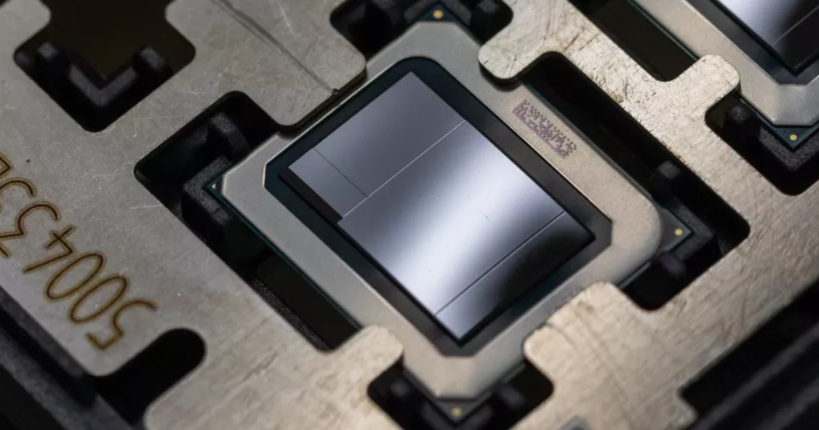
Meteor Lake processors will be made of four discrete chips (Intel calls them tiles), brought together through silicon vias (TSVs), connecting them to a base die. These will be the main compute tile, the graphics tile, the SoC tile, and the I/O tile. Intel uses its 3D Foveros chip-stacking packaging tech to connect them through that base silicon slice.
There was an initial delay to the mass production of its Intel 4 (nominally 7nm) process from 2022 to the start of 2023—which is going to be the lithography used for the Meteor Lake compute tile—and then Trendforce reported that orders for the 3nm TSMC process it claimed to be used for the GPU tile had been cut from Intel’s TSMC pre-order.
PC Watch (via Benchlife) reported Intel’s Boyd Phelps as saying “Meteor Lake is on schedule” at a media roundtable ahead of Hot Chips, presumably about these Trendforce rumors.
In February, Intel had said it was using an external N3 process for Meteor Lake and Arrow Lake. It is now being suggested to use a TSMC N5 node for Meteor Lake’s graphics. That would explain why a shift in N3 orders hasn’t affected the timing for Meteor Lake’s release, and if there’s one thing Intel needs to do with its processors, it is keep them coming on time.
Alongside rumored N5 lithography for its GPU tile, it is also said to be using a TSMC N6 process for the I/O and SoC tiles on the chip. With Intel manufacturing the 7nm compute tile, the 22nm base die for the packaging, and TSMC creating a further three tiles, you’ve got a contract manufacturer making most of the core components for an Intel chip.
That’s potentially a smart move by Intel, allowing it to separate the manufacturing demands and focus on the stuff it does well, namely the compute component.
Intel is set for a more detailed Meteor Lake presentation at Hot Chips 34 today, so fingers crossed, we’ll get some more juicy looks at Intel’s first consumer chiplet processor.
Looking further ahead, Intel says it will start to use the Universal Chiplet Interconnect Express (UCIe) standard for its processor designs in the latter half of the decade.
“We plan to use UCIe in later products than Arrow Lake,” says Phelps. That would potentially make the efficiency-focused Lunar Lake the first to use the new standard.
Intel is working on UCI, AMD, Arm, Microsoft, Google, TSMC, and many others, after Intel donated the open standard to the consortium as a whole and claims that such an open chiplet ecosystem could drive down costs, deliver higher performance, and lower power.